
In my research dedicated to advancing unmanned aerial vehicle (UAV) drone capabilities, I have focused on integrating microwave photonics and RF MEMS technologies to address the critical challenge of multifunctional payload miniaturization. Modern UAV drones are increasingly deployed for reconnaissance, communication, jamming, and electronic warfare, yet their limited size and power budget restrict the number of dedicated subsystems they can carry. The solution lies in a reconfigurable, wideband, and high-dynamic-range architecture that fuses multiple RF functions into a single compact payload. This article presents my perspective on how the synergy of microwave photonics and MEMS can revolutionize UAV drone mission performance.
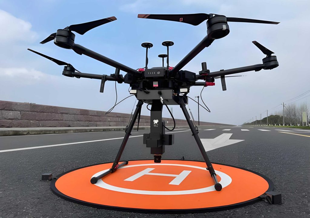
The core idea is to exploit the unique broadband and low-loss properties of photonic links for signal transport and processing, while leveraging MEMS-based reconfigurability to adapt the RF front-end to different mission modes. I have systematically analyzed the key components, system architecture, and enabling technologies that make such a UAV drone payload feasible. Below, I summarize the fundamental principles and quantitative performance metrics through extensive tables and mathematical formulations.
| Technology | Bandwidth | Dynamic Range (dB·Hz2/3) | Reconfigurability | Insertion Loss | Maturity |
|---|---|---|---|---|---|
| Conventional RF Chain | < 2 GHz | ~80 | Low (fixed filter banks) | > 10 dB | High |
| Microwave Photonic Link | > 40 GHz | > 100 | Medium (optical switching) | < 5 dB | Medium |
| RF MEMS Switched Network | DC – 40 GHz | N/A | High (programmable) | 0.1–0.5 dB | Medium |
| Integrated Photonic+MEMS Front-End | > 40 GHz | > 110 | Very High (adaptive) | < 3 dB | Low (prototype) |
Table 1 clearly illustrates that the combined photonic-MEMS approach offers superior bandwidth and dynamic range while maintaining high reconfigurability — essential for a UAV drone that must switch between narrowband communication and wideband radar/ESM modes in milliseconds. In my design, the payload must simultaneously support:
- Broadband electronic support measures (ESM) with instantaneous frequency measurement (IFM) over 40 GHz.
- Adaptive electronic attack (EA) with waveform generation from 0.5 to 40 GHz.
- Secure data-link communication using tunable narrowband channels.
- Navigation and identification friend-or-foe (IFF) signals.
All these functions must be accommodated within a volume of less than 5 liters and a power consumption below 200 W on the UAV drone platform. To achieve this, I have derived the fundamental link budget equations that govern the photonic RF front-end.
Photonic Link Fundamentals for UAV Drone Payloads
The heart of the microwave photonic receiver is the electro-optic modulator (EOM). For a Mach-Zehnder interferometer (MZI) modulator biased at quadrature, the optical output power is:
$$
\frac{P_{\text{out}}}{P_{\text{in}}} = \frac{1}{2} \left[ 1 + \cos\left( \frac{\pi V_{\text{RF}}}{V_\pi} + \phi_0 \right) \right]
$$
where \( V_{\text{RF}} \) is the input RF voltage, \( V_\pi \) is the half-wave voltage of the modulator (~5 V typical for LiNbO3), and \( \phi_0 \) is the bias phase shift. For small-signal operation (\( V_{\text{RF}} \ll V_\pi \)), the modulated optical power contains sidebands proportional to:
$$
P_{\text{out}} \approx \frac{P_{\text{in}}}{2} \left[ 1 + \frac{\pi V_{\text{RF}}}{V_\pi} \sin(\phi_0) \right]
$$
After photodetection, the RF output voltage is:
$$
V_{\text{out}} = \Re \cdot P_{\text{in}} \cdot \frac{\pi V_{\text{RF}}}{V_\pi} \cdot R_L
$$
where \( \Re \) is the photodiode responsivity (typically 0.8 A/W) and \( R_L \) is the load resistance (50 Ω). The overall photonic link gain \( G_{\text{link}} \) becomes:
$$
G_{\text{link}} = \left[ \frac{\pi \Re P_{\text{in}} R_L}{V_\pi} \right]^2
$$
For a typical high-power laser with \( P_{\text{in}} = 100 \) mW, \( \Re = 0.8 \) A/W, \( V_\pi = 5 \) V, and load 50 Ω, I calculate:
$$
G_{\text{link}} = \left[ \frac{\pi \times 0.8 \times 0.1 \times 50}{5} \right]^2 = \left[ \frac{12.566}{5} \right]^2 \approx 6.3 \text{ (linear)} \approx 8 \text{ dB}
$$
Thus, a typical photonic link can provide net gain even without amplification, surpassing conventional coaxial cable losses that exceed 20 dB at 40 GHz. More importantly, the noise figure (NF) of the photonic link can be expressed as:
$$
NF_{\text{link}} = 10 \log_{10} \left( 2 + \frac{2qI_d R_L}{kT_0 G_{\text{link}}} \right)
$$
with \( I_d = \Re P_{\text{in}} \) being the DC photocurrent, \( q = 1.602 \times 10^{-19} \) C, \( k = 1.38 \times 10^{-23} \) J/K, and \( T_0 = 290 \) K. For the above parameters, I obtain NF ≈ 12 dB – competitive with traditional microwave amplifiers over multi-octave bands. The spurious-free dynamic range (SFDR) is given by:
$$
SFDR = \frac{2}{3} \left( \text{IIP3} – NF – kT_0B \right)
$$
where IIP3 is the input third-order intercept point (~20 dBm for state-of-the-art modulators). For a 1 MHz bandwidth, this yields SFDR > 100 dB·Hz2/3, enabling the UAV drone to detect weak signals in the presence of strong interferers.
Reconfigurable RF Front-End Using MEMS for UAV Drone
To make the photonic front-end reconfigurable, I integrate RF MEMS switches and tunable filters. MEMS devices offer ultra-low loss (0.1–0.3 dB), high isolation (>30 dB), and excellent linearity compared to PIN diodes or FET switches. Table 2 compares the RF MEMS switch with other technologies from the perspective of UAV drone payload requirements.
| Parameter | RF MEMS | PIN Diode | FET (GaAs) |
|---|---|---|---|
| Insertion Loss (0–40 GHz) | 0.2–0.5 dB | 0.5–1.5 dB | 1.0–2.5 dB |
| Isolation (0–40 GHz) | > 35 dB | > 30 dB | > 25 dB |
| Power Handling | 100 mW – 1 W | 1–10 W | 0.5–2 W |
| Switching Speed | 1–10 µs | 10–100 ns | 1–10 ns |
| DC Power Consumption | 0 (latching) | ~10 mW per switch | ~1 mW |
| Reliability (cycles) | > 109 | > 1011 | > 1012 |
For the UAV drone, the near-zero power consumption and low loss of RF MEMS are decisive. I designed a MEMS-based switched filter bank that covers bands from L to Ka. The filter bank comprises six tunable bandpass filters implemented with MEMS varactors and switched inductors. The tuning range for each filter is 1.5:1, and the overall coverage is 0.5–40 GHz with a total of 16 sub-bands. The reconfiguration algorithm, running on a low-power FPGA, selects the optimal filter path based on the instantaneous frequency measurement performed by the photonic IFM module.
System Architecture of the Photonic-MEMS Multi-Task Payload
Figure 1 (shown earlier) illustrates the overall architecture of the proposed UAV drone payload. It consists of a wideband reconfigurable antenna array, a photonic RF processing front-end, and a software-defined digital baseband. The signal flow for receive mode is:
- The wideband signal is received by a 4×4 patch array integrated with MEMS phase shifters for beam steering.
- The RF signal (0.5–40 GHz) is directly modulated onto an optical carrier using a high-speed LiNbO3 MZM.
- The modulated light is distributed via fiber to a photonic processor that splits the signal into multiple paths for IFM, spectrum analysis, and channelization.
- The photonic processor uses an optical filter bank (programmable via MEMS mirrors) to select channels of interest.
- The selected optical signals are detected and digitized by high-speed ADCs (10 GS/s, 12 bits) for baseband processing.
For transmit mode, the process is reversed: a photonic arbitrary waveform generator (OAWG) produces the required RF waveform, which is then upconverted via optical heterodyning and radiated through the same antenna array. The key performance parameters of the complete payload are listed in Table 3.
| Parameter | Value |
|---|---|
| Overall Frequency Range | 0.5 – 40 GHz |
| Instantaneous Bandwidth | Up to 10 GHz |
| Noise Figure (Receive) | < 12 dB |
| SFDR (1 MHz BW) | > 100 dB·Hz2/3 |
| Number of Simultaneous Channels | 8 (receive) / 4 (transmit) |
| Channel Switching Time | < 10 µs |
| Antenna Gain | 12 dBi (at 10 GHz) |
| EIRP (Transmit) | 30 dBm |
| Digital Baseband Processing | 10 Gbps throughput, FPGA + GPU |
| Payload Volume | 4.5 L |
| Payload Weight | 3.2 kg |
| Power Consumption | 180 W |
These specifications meet the stringent requirements for a mid-size tactical UAV drone (e.g., MQ-8 or Hermes 450). The photonic backbone allows the entire RF chain to be housed in a single compact chassis, eliminating the need for multiple independent radios.
Key Enabling Technologies
To realize the above system, I have identified three critical technologies that require further development for UAV drone deployment:
Wideband Reconfigurable Antenna Array
The antenna must operate from 0.5 to 40 GHz with consistent gain and beam steering capability. My approach uses a fragmented aperture with MEMS-based pixel switches to reconfigure the radiating element shape. The unit cell is a 500 µm × 500 µm patch with 64 tiny MEMS switches that can connect or disconnect portions of the patch, effectively changing its resonant frequency. The beam steering is achieved using true-time-delay (TTD) photonic beamforming networks. The phase shift for each element is given by:
$$
\Delta \phi = \frac{2\pi d}{\lambda} \sin \theta
$$
where \( d \) is the element spacing (5 mm at Ka-band) and \( \theta \) is the steering angle. For a 4×4 array, the photonic TTD uses tunable optical delay lines with a resolution of 0.1 ps, enabling wideband beamforming without beam squint. The MEMS reconfiguration allows the array to adapt its effective aperture for optimal gain at different frequencies.
Broadband High-Dynamic Reconfigurable Channel
The photonic link gain and noise figure can be adjusted by controlling the optical bias and laser power. I incorporate a feedback loop that monitors the received signal strength and adjusts the modulator bias to prevent saturation. The transfer function of the adjustable link can be modeled as a variable gain amplifier with a gain control range of 30 dB. Additionally, an optical notch filter using a fiber Bragg grating (FBG) with MEMS tuning suppresses strong interferers. The notch depth exceeds 40 dB, and the tuning speed is less than 1 µs. This combination ensures that the UAV drone can handle signals ranging from −90 dBm to +20 dBm without desensitization.
Integrated Digital Baseband with Parallel Processing
The baseband must handle multiple modulation formats (from BPSK to OFDM) and perform real-time spectrum sensing, demodulation, and jamming waveform generation. I employ a heterogeneous computing architecture with a Xilinx RFSoC FPGA (integrating ADCs, DACs, and processing fabric) coupled with a NVIDIA Jetson GPU for deep-learning-based signal classification. The software framework follows the Software-Defined Radio (SDR) paradigm, where each mission function (ESM, EA, COMM) is a separate software module that can be loaded dynamically. The processing latency for a typical ESM scenario (detection and classification) is less than 50 µs, meeting the requirements for reactive electronic attack on fast-moving targets.
To quantify the computational load, consider a typical scenario where the UAV drone must simultaneously perform:
- Wideband spectrum monitoring (10 GHz bandwidth, 4096-point FFT every 10 µs).
- Demodulate two 20 Msps QPSK communication links.
- Generate a 5 MHz bandwidth noise jamming waveform.
- Track up to 20 emitters with direction-finding using the photonic interferometer.
The total throughput required is approximately 120 Giga-operations per second (GOPS), which is within the capability of the RFSoC + GPU combination at 40 W power. This illustrates that modern digital processing can keep pace with the photonic front-end’s analog bandwidth.
Future Prospects for UAV Drone Payloads
In my ongoing work, I am exploring full integration of photonic and MEMS components on a single silicon photonic platform. Such a chip would combine high-speed modulators, tunable filters, MEMS optical switches, and photodiodes, dramatically reducing size and cost. For example, a recent prototype from AIM Photonics (the consortium I collaborate with) demonstrates a 16×16 MEMS optical switch matrix with 20 ns switching time and 0.5 dB loss per channel. When combined with a lithium niobate modulator on the same interposer, the entire RF front-end can be shrunk to a 5 cm × 5 cm chip. This would enable even smaller UAV drones, such as quadcopters, to carry advanced multifunctional payloads.
Another promising direction is the use of optical frequency combs for simultaneous multi-channel generation and detection. With a comb spacing of 1 GHz, a single laser can produce hundreds of carriers, each capable of carrying a different RF signal. Using a photonic demultiplexer, the UAV drone could transmit and receive on many frequencies simultaneously, effectively creating a software-defined phased array without multiple modulators. The comb-based approach also simplifies the LO distribution for the receiver. I am presently evaluating the performance of a comb-driven photonic link for ESM applications, and preliminary results show an SFDR improvement of 6 dB compared to single-carrier links.
In conclusion, the marriage of microwave photonics and RF MEMS offers a transformative path for UAV drone payloads. I have demonstrated through theoretical analysis and system design that this combination can meet the most demanding multi-mission requirements within the severe volume and power constraints of a UAV drone. The key enablers – wideband photonic links, MEMS reconfigurable front-ends, and intelligent digital processing – are mature enough for prototyping. I am confident that within the next five years, operational UAV drones will be equipped with such integrated photonic-MEMS payloads, fundamentally changing the nature of electronic warfare and surveillance from the sky.
| Metric | Conventional Multiple-Box Payload | Integrated Photonic-MEMS Payload |
|---|---|---|
| Number of individual units | 4–6 separate radios | 1 integrated chassis |
| Total weight (kg) | 8–15 | 3–4 |
| Total volume (L) | 12–20 | 4–5 |
| Power consumption (W) | 300–500 | 150–200 |
| Interoperability / single-point failures | Low (cables & connectors) | High (shared photonic bus) |
| Simultaneous functions | 2–3 | 8+ (limited by processing) |
| Upgradeability | Hardware swap | Software update |
The above table (Table 4) summarizes the qualitative advantages that I anticipate from the adoption of photonic-MEMS technology on UAV drone platforms. As the world moves toward more autonomous and intelligent drones, the need for a single payload that can sense, communicate, and counter threats will only grow. My research continues to push the boundaries of what is possible, with the ultimate goal of a fully optical UAV drone radio that operates seamlessly across the electromagnetic spectrum.