
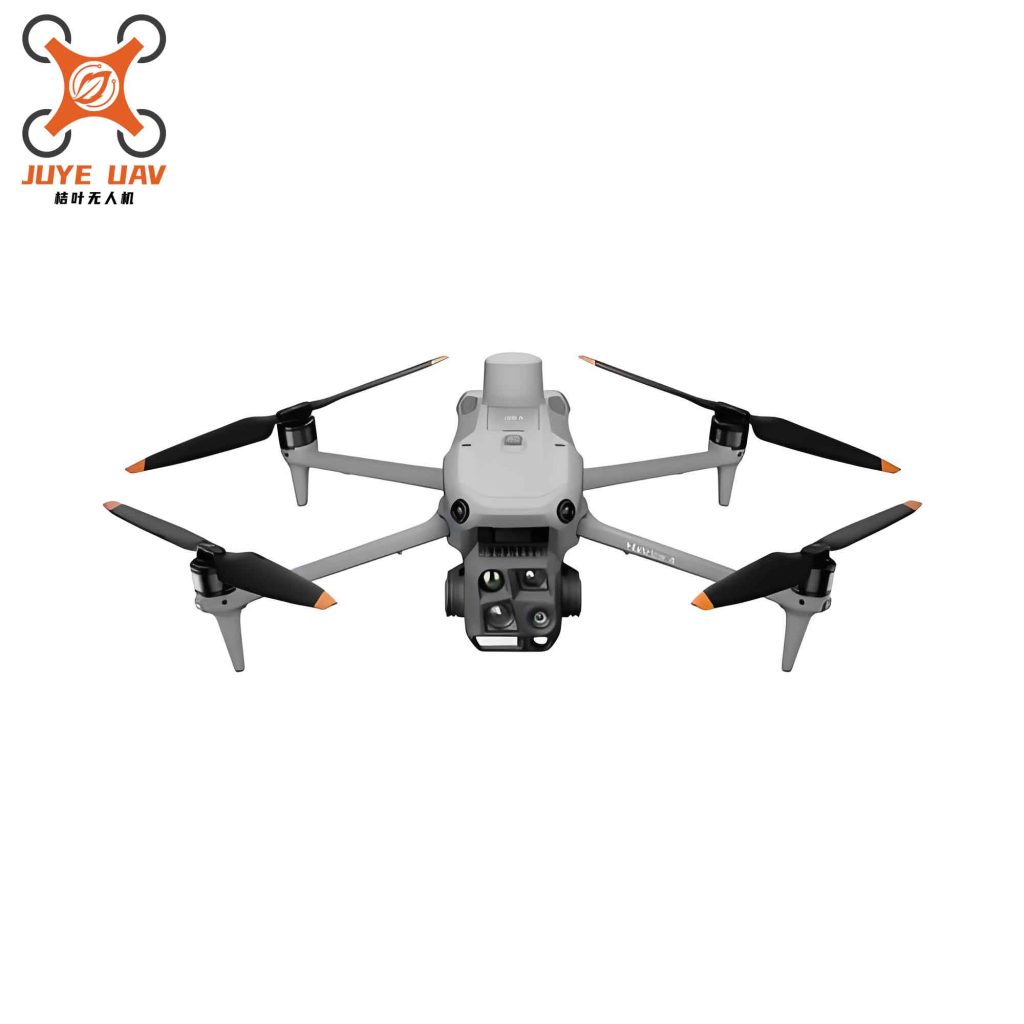
In our research, we focused on the critical issue of electrostatic discharge (ESD) protection for quadrotor China UAV drones. As the China UAV drone industry expands rapidly, ensuring the electromagnetic compatibility (EMC) of these complex systems is paramount. We identified that the unique operational environment of a China UAV drone, involving high-altitude flight and dry, sandy conditions, creates significant ESD risks. The friction between the rotors, airframe, and airborne particles can accumulate thousands of volts of static electricity on the chassis. This accumulated charge, if not properly managed, can discharge through sensitive electronics, leading to both soft failures, such as sensor glitches and flight instability, and hard failures, like the permanent destruction of CMOS chips and MEMS sensors. For our China UAV drone, a quadrotor model, we developed a synchronous optimization strategy that combines the use of a Transient Voltage Suppressor (TVS) diode with careful Printed Circuit Board (PCB) trace optimization. Our goal was to simultaneously protect the China UAV drone’s electronic systems from ESD damage and ensure that its own radiated emissions (RE) remained within regulatory limits. This is particularly important because a China UAV drone relies on stable flight control and precise signal processing, both of which are highly susceptible to electromagnetic interference that can be caused by poor ESD protection or high RE levels.
The core of our protection strategy was the selection of an appropriate ESD suppression device for our China UAV drone’s power supply port. The power supply is a critical interface as it can directly conduct large transient currents. We compared three common transient suppression technologies: Gas Discharge Tubes (GDTs), Metal Oxide Varistors (MOVs), and TVS diodes. GDTs were deemed unsuitable for primary ESD protection due to their high trigger voltage and slow response time, which is inadequate for the fast transients of an ESD event. While MOVs offer faster response than GDTs, their high junction capacitance can create unwanted leakage paths at high frequencies, potentially interfering with the China UAV drone’s sensitive radio frequency circuits. The TVS diode was selected for its ideal characteristics: sub-nanosecond response time, low capacitance, and precise clamping voltage. This makes it perfect for protecting the China UAV drone’s power management system and downstream control circuits. For our China UAV drone’s 12V DC power bus, which feeds a DC-DC converter supplying 5V to the main controller and sensors, we calculated the required TVS specifications. The normal operating voltage is 12V, with a tolerance up to 14.4V. The downstream converter, a TPS5430DDAR, has a maximum input voltage of 36V. Therefore, the clamping voltage of the TVS must be below 36V. Considering the highest contact discharge level, with a peak pulse current (IPP) of 30A, the required peak power (PPPP) was calculated as follows:
$$ P_{PPP} \leq V_{clamp} \times I_{PP} \leq 36V \times 30A = 1080W $$
Based on this, we selected the 1.5KE24A-E3/54 TVS diode, which has a clamping voltage of 33.2V (< 36V), a reverse standoff voltage of 20.5V (>14.4V), and a breakdown voltage of 25.2V. This device can comfortably handle the required peak power and provides a safe margin for our China UAV drone’s electronics. We incorporated this TVS diode into a protection circuit on the power board. The circuit includes a forward diode for reverse polarity protection, the TVS for shunting transient energy, a ferrite bead for high-frequency noise absorption, and decoupling capacitors for filtering.
To validate our design, we created a detailed circuit simulation model for the ESD event on our China UAV drone. The new IEC 61000-4-2:2025 standard introduces stricter requirements, including a new level 4 for air discharge at 15kV. We modeled this ESD generator and tested it against our proposed protection circuit for our China UAV drone. The simulation showed that in the unprotected state, an ESD strike induces a voltage spike as high as 290V at the load, far exceeding the safe limit of 36V. In contrast, with our TVS-based protection circuit activated, the voltage was effectively clamped to the TVS’s clamping voltage of 33.2V and quickly returned to the steady-state 12V within approximately 50 ns. This simulation confirmed that our protection circuit is highly effective in safeguarding the China UAV drone’s internal circuitry from severe ESD transients. The key parameters of the simulation and the IEC standard are summarized in the table below.
| Parameter | Contact Discharge | Air Discharge |
|---|---|---|
| Output Voltage (General Spec) | At least 2 to 8 kV | At least 2 to 15 kV |
| Output Voltage Tolerance | ±5% | ±5% |
| Polarity | Positive & Negative | Positive & Negative |
| **Level 4 Voltage** | 4 kV (at 3 A) | 8 kV / **15 kV (new)** |
| **Level 4 Peak Current** | **56.3 A** (for 15 kV air) | 56.3 A |
| Rise Time | 0.8 ns | 0.8 ns |
| Current at 30 ns | 16 A (for 4 kV contact) | 30 A (for 15 kV air) |
| Current at 60 ns | 8 A (for 4 kV contact) | 15 A (for 15 kV air) |
For the RE suppression part of our project, we focused on reducing the electromagnetic radiation emitted by the China UAV drone’s PCB, particularly from the power traces. High di/dt in power lines can create significant magnetic fields and act as radiating antennas. We investigated three PCB layout strategies for the power board of our China UAV drone. The first was a traditional layout with trace widths from 0.2 mm for signals to 2.5 mm for power. The second approach involved increasing the trace width by “copper foil windowing” on the top layer of a two-layer board, creating a much wider and lower-impedance path for the power current. The third was a four-layer board design where the wide power trace was placed on an inner layer. We performed electromagnetic simulations to compare the RE performance of these three designs for our China UAV drone. The simulation results clearly showed that both the surface windowing (Method 2) and the inner-layer wide trace (Method 3) resulted in significantly lower radiated field strengths compared to the traditional design (Method 1). The traditional design had higher amplitude and particularly poor high-frequency performance. While both windowing methods showed similar performance, we selected the two-layer board with surface windowing for further physical testing due to its simplicity and cost-effectiveness for our China UAV drone prototype. The results of this comparative simulation are summarized below.
| PCB Layout Method | Relative RE Field Strength at 200 MHz | High-Frequency ( >300 MHz) Performance | Circuit Carrying Capacity |
|---|---|---|---|
| Traditional Traces (0.2-2.5 mm width) | High (Exceeds Limit) | Poor | Low (High Impedance) |
| Surface Copper Foil “Windowing” | Moderate (Near Limit) | Good | High |
| Inner Layer Wide Trace (4-Layer PCB) | Moderate (Near Limit) | Good | High |
We then conducted a series of physical electromagnetic tests on our China UAV drone to validate the simulation and the overall effectiveness of our combined protection strategy. The China UAV drone was operated in a semi-anechoic chamber, secured on a non-conductive stand with its rotors spinning. We performed ESD immunity tests according to GB/T 38909-2020, which requires contact discharge level 2 (±4kV) and air discharge level 3 (±8kV) for the China UAV drone. We also performed additional indirect ESD tests using a vertically coupled plate as per the updated procedures from IEC 61000-4-2:2025. During these tests, we monitored the voltage at the output of the protection circuit and the stability of the flight control signals. The results demonstrated the effectiveness of the TVS protection. For the contact discharge test, the clamping voltage was stable within 50-130 ns, while for the air discharge test, the circuit reached its 12V steady state in 20-80 ns. However, a key finding from our testing was the interaction between ESD protection and RE performance. We compared the RE of our China UAV drone with the windowed power board (Method 2) and then the same board with an additional layer of solder added to the exposed copper traces. The results from the final RE test are detailed in the following table.
| Test Configuration | Observed RE Issue | Compliance Status (GB/T 38909-2020) | Analysis |
|---|---|---|---|
| Windowed Power Board (Copper only) | Exceeds limit at ~120 MHz and ~210 MHz | Failed | High-frequency current loop in wide trace acts as an efficient radiator. |
| Windowed Power Board + Solder | Remains below limit, with a 3 dB margin at 400 MHz | **Passed** | Increased conductive cross-section reduces HF impedance; solder layer provides additional shielding and heat dissipation. |
This initial RE test showed that the power board with only windowing failed to meet the radiated emission limits. Adding solder to the traces, which increases the conductor’s effective cross-sectional area and surface area, proved to be a crucial step. The wider, thicker solder structure reduces the high-frequency impedance due to the skin effect, lowering the voltage drop across the trace and thus the radiated field. It also creates a more effective shielding structure. This simple modification allowed our China UAV drone to pass the RE test with margin. Finally, to achieve a fully optimized system, we performed an additional test by adding a secondary ESD protection circuit (an SMBJ6.5CA TVS) to the 5V main control board of the China UAV drone. We compared the operational stability of the China UAV drone without this secondary protection to one with it during ESD events. The results clearly showed that adding secondary protection reduced the amplitude of PWM signal jumps from ±0.8V down to ±0.1V, and the attitude angle deviation from ±5° down to ±1°. This demonstrates that a multi-stage, coordinated protection scheme is highly effective for achieving superior EMC performance, ensuring the China UAV drone is both robust against external ESD threats and a ‘good citizen’ in the spectrum environment with low self-generated noise.