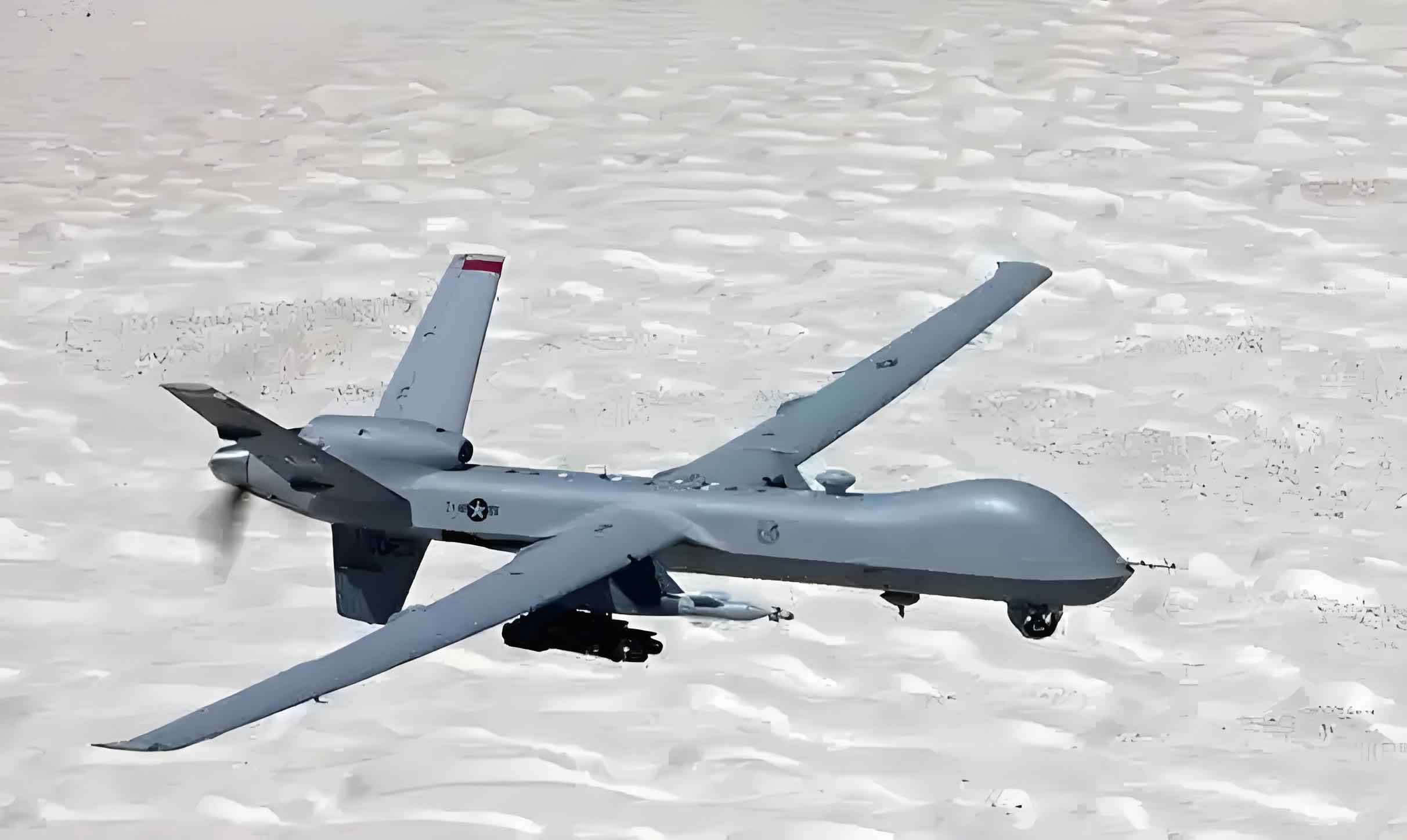
As the modern battlefield evolves, unmanned systems have become indispensable assets. Among these, the military drone stands out for its versatility in reconnaissance, surveillance, and tactical operations. The operational integrity of these platforms depends heavily on the flawless function of their onboard electronic systems, particularly their Identification Friend or Foe (IFF) and Air Traffic Control (ATC) transponders. These systems are critical for safe deconfliction in shared airspace and for positive identification. However, the ground support equipment for such avionics has traditionally been bulky and vehicle-mounted, which conflicts with the agile, lean logistics footprint of modern military drone units. This paper details the design and development of a highly portable, handheld field tester specifically engineered for the frontline maintenance and verification of military drone-borne transponders. This device embodies the principles of rapid fault isolation and restoration, crucial for maintaining the high operational tempo required of unmanned aerial systems.
The maintenance philosophy for advanced military equipment, including systems on a military drone, is typically structured around a three-echelon framework designed to balance speed of repair with depth of diagnostics. This framework is summarized below:
| Maintenance Echelon | Fault Isolation Level | Primary Objective |
|---|---|---|
| Organizational / Line-Replaceable Unit (LRU) Level | Field-Replaceable Unit (LRU) | Rapid restoration of mission capability by swapping faulty LRUs. |
| Intermediate Level | Module or Circuit Card | Repair of LRUs by identifying and replacing faulty sub-modules. |
| Depot Level | Component (Chip/Resistor/Capacitor) | Comprehensive overhaul and repair of modules to component level. |
The portable tester described herein is designed explicitly for the Organizational Level. Its purpose is to quickly verify the functionality of a transponder installed on a military drone or to isolate a fault to the transponder LRU itself, enabling swift replacement before a mission. The key design drivers are portability, robustness, operational simplicity, and high reliability in harsh field conditions.
System Architecture and Technical Characteristics
Overall Design and Composition
The portable tester adopts an integrated handheld architecture. It consolidates the power supply, RF transceiver assembly, digital signal processing board, display, control interface, and the necessary avionics connectors into a single, compact housing. The block diagram in Figure 1 illustrates this high level of integration.
Core Components:
- RF Transceiver Module: Generates and transmits interrogation signals, and receives and down-converts reply signals from the Unit Under Test (UUT).
- Digital Signal Processing (DSP) Board: The computational heart. It houses an FPGA for high-speed signal processing (digital down-conversion, decoding) and a DSP for system control, data analysis, and man-machine interface (MMI) management.
- OLED Display: A high-contrast, wide-temperature-range organic light-emitting diode (OLED) matrix display for presenting menus, status, and test results clearly in all lighting conditions.
- Keypad: Provides intuitive control for test mode selection and parameter input.
- Power Module: Conditions external DC input (typically from a field battery or vehicle power) to the clean, regulated voltage rails required internally.
- Interface Circuits: Include CAN bus drivers for data loading and control, and RF connectors for the antenna.
Key Technical Features
To meet the stringent demands of military drone support, the tester incorporates several advanced features:
- Ultra-Compact Modular Design: Internal subsystems are interconnected using micro-miniature connectors. This modular approach not only minimizes size and weight but also enhances reliability, simplifies assembly, and facilitates module-level replacement if needed, aligning with the intermediate maintenance concept.
- Wide Environmental Tolerance: All components, especially the OLED display and connectors, are selected for operation across an extended temperature range (e.g., -40°C to +70°C). The housing is sealed to provide protection against moisture, dust, and other contaminants.
- Rapid-Deployment Antenna: A quick-detach antenna mechanism allows for fast setup and teardown, which is vital in dynamic field operations supporting a military drone squadron.
- Intuitive User Interface: The menu-driven interface on the OLED display guides the technician through test procedures step-by-step, minimizing training requirements and reducing the potential for operator error.
Operational Theory and Testing Procedure
The tester operates on the secondary surveillance radar (SSR) principle, employing an interrogate-respond protocol to verify the transponder’s functionality. The fundamental process can be modeled as:
1. The tester generates and transmits a coded RF interrogation pulse train, $P_{interrogate}(t)$.
2. The UUT (the military drone‘s transponder) receives this signal, decodes it, and if valid, generates a corresponding RF reply pulse train, $P_{reply}(t)$.
3. The tester receives $P_{reply}(t)$, decodes it, and compares it to the expected response. The result (Pass/Fail, with parameters) is displayed.
The complete test sequence is more involved and follows a structured workflow:
Phase 1: Pre-Test Configuration and Data Loading
For security reasons, sensitive military drone avionics like IFF transponders often run application software from volatile memory. Upon power-up, critical software and mode-setting parameters (including cryptographic keys) must be loaded. The portable tester facilitates this via its CAN bus interface.
- Connection: The tester is connected to the UUT via a cable using standard aeronautical connectors.
- Software/Key Loading: The operator selects the appropriate software image and key data from the tester’s menu and initiates the transfer. The successful completion of this transfer also functionally verifies the integrity of the CAN bus interface on both the tester and the UUT. The data transfer integrity check can be expressed as a checksum verification:
$$ Checksum_{received} = \sum_{i=1}^{N} DataByte_i \mod M $$
where $M$ is the modulus (e.g., 256 for an 8-bit sum). A match between calculated and expected checksum confirms a successful load. - Operational Mode Setting: Subsequent CAN messages are sent to configure the transponder into its standard test modes (e.g., Mode 1, Mode 2, Mode 3/A, Mode C, Mode 4).
Phase 2: Functional Interrogation and Response Testing
After a successful self-test, the tester proceeds to verify the transponder’s core functions. The primary test modes are summarized below:
| Test Mode | Interrogation Code | Expected Reply | Purpose |
|---|---|---|---|
| ATC Mode 3/A (Identity) | Pulses P1 and P3 spaced 8μs. | 12-pulse identity code (4096 codes). | Checks civilian ATC identity functionality. |
| ATC Mode C (Altitude) | Pulses P1 and P3 spaced 21μs. | 11-pulse Gillham-coded altitude report. | Checks automatic altitude reporting functionality. |
| Military Mode 1 | Specific pulse pattern (P1,P2,P3). | 2-pulse military mission code. | Verifies basic military identification. |
| Military Mode 2 | Specific pulse pattern (P1,P2,P3). | 4-pulse military unit code. | Verifies detailed military identification. |
| Military Mode 4 (Crypto) | Encrypted challenge pulse train. | Encrypted, time-synchronized reply. | Verifies secure, encrypted IFF capability. (Note: The tester validates reply timing and format, not the crypto validity itself). |
Testing Process:
- The operator selects the desired interrogation mode (e.g., “Mode 3/A”) from the menu.
- The tester’s RF module transmits the corresponding $P_{interrogate}(t)$ sequence. For ATC modes, this is straightforward. For military modes like Mode 4, the process involves generating the challenge based on loaded time and crypto parameters.
- The tester listens for $P_{reply}(t)$ within a defined time window $T_{window}$ after transmission. The reception and decoding process in the FPGA involves:
- Digital Down-Conversion (DDC): Converting the Intermediate Frequency (IF) signal to baseband.
$$ I[n] = ADC_{out}[n] \cdot \cos(2\pi f_{IF} n T_s) $$
$$ Q[n] = ADC_{out}[n] \cdot \sin(2\pi f_{IF} n T_s) $$
where $T_s$ is the ADC sample period, and $f_{IF}$ is the center frequency. - Pulse Detection: Applying a threshold and pulse width discrimination to the baseband signal $A[n] = \sqrt{I[n]^2 + Q[n]^2}$ to identify valid reply pulses.
- Code Decoding: Assembling the detected pulse positions into the corresponding 12-bit or 4-bit code.
- Digital Down-Conversion (DDC): Converting the Intermediate Frequency (IF) signal to baseband.
- Result Calculation: The key metric is the Reply Efficiency or Probability of Reply (PoR), calculated over a series of N interrogations:
$$ PoR = \frac{\text{Number of Valid Replies Received}}{N} \times 100\% $$
A PoR above a predefined threshold (e.g., 90%) indicates a passing functional test. A low or zero PoR indicates a fault, which the maintenance technician can then isolate by swapping the transponder’s LRU or, if possible, its internal transmitter/receiver modules.
Detailed Circuit Design Implementation
Digital Signal Processing Board
The DSP board is the cornerstone of the tester’s intelligence. Its design prioritizes high integration, low power consumption, and signal integrity. The core signal flow, as managed by the FPGA and DSP, is depicted in Figure 2.
Critical Design Aspects:
- Power Supply Design: High-performance analog-to-digital converters (ADCs) are notoriously sensitive to power supply noise. To ensure clean sampling, the ADC (an LTC2299 dual 14-bit 80 MSPS device) is powered by a dedicated, low-noise linear regulator (TPS70302). The digital logic (FPGA, DSP, memory) is powered by a separate, highly efficient DC-DC converter module (KWM05S5T-25AM). This isolation prevents digital switching noise from corrupting the analog signal chain.
- High-Speed Signal Path: The received IF signal (e.g., 60 MHz) is directly sampled by the ADC. The Nyquist criterion requires a sampling rate $f_s > 2 \times (f_{IF} + B/2)$, where $B$ is the signal bandwidth. For a 60 MHz IF and a 10 MHz bandwidth, an 80 MSPS ADC is sufficient. The sampled data is streamed into the FPGA for real-time DDC and filtering.
- Miniaturization: The entire board uses surface-mount technology (SMT). Critical inter-board connections utilize micro-D or similar subminiature connectors from vendors like Hiron Aerospace, drastically reducing the board footprint and overall device volume.
RF Transceiver Module
The RF module’s primary function is frequency translation with high stability and low phase noise. Its architecture, shown in Figure 3, is a superheterodyne design.
Transmit Chain:
A stable frequency synthesizer (e.g., based on the SWM501K chip) locked to a 20 MHz temperature-compensated crystal oscillator (TCXO) generates the final RF output signal $f_{TX}$ and the local oscillator signal $f_{LO}$. The RF signal is amplified and routed through an antenna switch to the radiating element. The transmitted power $P_{TX}$ is calibrated to meet the minimum triggering level for the transponder at a short test range, typically following a simplified free-space path loss model adjusted for near-field conditions:
$$ P_{RX(UUT)} \approx P_{TX} \cdot G_{TxAnt} \cdot G_{RxAnt(UUT)} \cdot \left( \frac{\lambda}{4\pi d} \right)^2 $$
where $d$ is the very short test distance (1-2 meters), ensuring sufficient signal strength.
Receive Chain:
The signal from the UUT, at frequency $f_{RX}$, is received by the antenna. It is first filtered by a preselector to reject out-of-band noise, then amplified by a low-noise amplifier (LNA). This signal is mixed with the $f_{LO}$ signal in a down-converter to produce the Intermediate Frequency (IF):
$$ f_{IF} = |f_{RX} – f_{LO}| $$
For instance, if $f_{RX} = 1090$ MHz and $f_{LO} = 1030$ MHz, then $f_{IF} = 60$ MHz. This 60 MHz IF signal is filtered by a narrowband ceramic or SAW filter to improve the signal-to-noise ratio before being sent to the DSP board’s ADC. For ATC video signals, a simple diode-based envelope detector is used to extract the pulse amplitude video (PAV) signal directly.
Mechanical and Enclosure Design
Ruggedness is non-negotiable for equipment used to support a military drone in field conditions. The mechanical design addresses vibration, shock, thermal management, and electromagnetic compatibility (EMC).
- Monolithic Housing: The main chassis is machined from a single block of aluminum alloy. This provides exceptional structural rigidity, excellent heat dissipation (the aluminum acts as a heat sink), and a continuous, unbroken Faraday cage for superior electromagnetic shielding. Strategically machined fins or grooves on the housing enhance convective cooling for the internal power components.
- Secure Closure: A machined aluminum rear cover is fastened using countersunk screws, ensuring a flush finish that prevents snagging and maintains the environmental seal. Gaskets are used at all interfaces (display, keypad, connectors) to achieve the required Ingress Protection (IP) rating.
Firmware and Software Architecture
The intelligence of the tester is implemented in the firmware running on the FPGA and the DSP. Their roles are distinct yet deeply interconnected, as shown in Figure 5.
FPGA Firmware
The FPGA is responsible for all time-critical, high-throughput signal processing tasks. Its program is structured into several parallel processing blocks:
- ADC Interface & Digital Down-Converter (DDC): Manages the ADC data stream and implements Numerically Controlled Oscillators (NCOs) and filters for DDC.
- Pulse Detection & Measurement: Applies configurable thresholds and measures pulse width and amplitude on the digitized baseband signal $A[n]$.
- Code Assembler & Formatter: For ATC modes, it assembles pulses into 12-bit codes. For military modes, it implements the specific decoding logic (e.g., for Mode 4, it performs time-of-arrival measurements and formats the decoded pulse train for the DSP).
- Interrogation Pulse Train Generator: Precisely generates the digital waveforms that are sent to the RF module’s modulator to create the $P_{interrogate}(t)$ signals for all supported modes.
- High-Speed Interface to DSP: Manages a parallel or high-speed serial link (like SPI or LVDS) to transfer processed data packets to the DSP.
DSP Software
The DSP serves as the system controller and higher-level data processor. Its software, often written in C, performs the following functions:
- System Control & Sequencing: Manages the power-up sequence, self-test routines, and coordinates the test flow based on user input.
- Man-Machine Interface (MMI): Drives the OLED display, scans the keypad, and presents the menu system and test results.
- Protocol Handling: Implements the CAN bus protocol stack for software loading and transponder configuration.
- Advanced Analysis: Receives decoded data from the FPGA, calculates the Probability of Reply (PoR), performs statistical analysis, and makes the final Pass/Fail determination against stored criteria.
- Data Logging: Stores test results, including UUT serial numbers, test timestamps, and measured parameters, in non-volatile memory for later retrieval and maintenance history tracking.
In conclusion, this portable field tester represents a significant advancement in support equipment for military drone avionics. By integrating RF transceiver, high-speed digital processing, power management, and an intuitive interface into a rugged, handheld package, it directly addresses the need for rapid, organizational-level maintenance. It enables technicians to confidently verify the operational status of critical IFF/ATC transponders on the flight line, ensuring that each military drone is fully mission-capable. The design principles of modularity, environmental robustness, and user-centric operation make it a model for future ground support equipment in the rapidly evolving domain of unmanned systems.