
In my work on UAV drones, I have always been challenged by the stringent requirements of lightweight, miniaturization, and high performance for photoelectric payload systems. These UAV drones demand a controller that can handle both multitask management and servo stabilization control with low power consumption and small physical footprint. Traditional solutions using separate PowerPC and DSP processors with serial communication often suffer from large size, high power consumption, and limited communication bandwidth. To address these issues, I designed a photoelectric payload controller based on the ARM+DSP dual-core heterogeneous processor OMAPL138 from Texas Instruments. This design leverages the strengths of both cores: the ARM9 manages system tasks and communication, while the C674x DSP performs intensive real-time control algorithms. By utilizing shared memory and SysLink inter-core communication, I achieved efficient and reliable data exchange, significantly improving the controller’s performance for UAV drones.
The OMAPL138 processor integrates an ARM926EJ-S core and a TMS320C674x DSP core on a single chip. The ARM core is a 32-bit RISC CPU with Jazelle technology, running at up to 375 MHz, while the DSP core is a 32-bit VLIW architecture capable of both fixed-point and floating-point operations at up to 456 MHz. This dual-core architecture allows me to offload complex control algorithms to the DSP while the ARM handles higher-level system tasks such as command parsing, sensor management, and network communication. The processor also provides rich peripheral interfaces including EMIFA, EMIFB, USB, Ethernet, SPI, and I2C, which are essential for connecting various sensors and actuators in UAV drones.
To enable seamless collaboration between the two cores, I adopted the SysLink software package. SysLink provides a standardized inter-processor communication (IPC) framework that supports message queues (MessageQ) and ring buffers (RingIO) over shared memory. For my controller, I partitioned the 128 MB DDR2 memory as shown in Table 1. The ARM core runs a Linux operating system, while the DSP core runs the SYS/BIOS real-time operating system. Shared memory regions SR0, SR1, and SR2 are allocated for message passing and data streaming between the cores.
| Region | Start Address | Size (MB) | Owner | Purpose |
|---|---|---|---|---|
| ARM Private | 0xC0000000 | 32 | ARM | Linux kernel, apps |
| DSP Private | 0xC2000000 | 64 | DSP | DSP program, data |
| SR0 (Shared) | 0xC6000000 | 4 | Both | Message queues |
| SR1 (Shared) | 0xC6400000 | 6 | Both | ARM → DSP data |
| SR2 (Shared) | 0xC6A00000 | 6 | Both | DSP → ARM data |
During the development phase, debugging the dual-core system was critical. I employed a combined GDB and CCS debugging method. On the ARM side, I used GDB server running on the target board, while on the DSP side, I used CCS via JTAG. The static debugging interface allowed me to set breakpoints in both cores simultaneously and observe the execution flow. The typical debugging sequence involves: (1) ARM loads the SysLink module; (2) ARM starts the DSP program using slaveloader; (3) PC loads DSP debug symbols via CCS; (4) ARM launches GDB server; (5) PC connects to GDB server and loads ARM debug symbols; (6) breakpoints are set in both environments. This approach greatly improved the development efficiency for my UAV drones controller.
The overall block diagram of my controller is illustrated in the figure below. Although I cannot reference the figure number, the system includes a NAND Flash (K9F4G08U0D, 512 MB, 8-bit) for bootloader and file system, a DDR2 (MT47H64M16HR, 128 MB, 16-bit, 400 MHz) for runtime memory, an 8-channel RS422 serial port expansion chip TL16CP754CIPM with EMIF interface for high-speed communication, GPIOs for powering thermal imagers and lasers, a resolver-to-digital converter AD2S80 for angle feedback, a 16-bit 8-channel ADC AD7606 for tachometer and gyro signals, and a PWM output stage for motor control. The interfaces include JTAG, console RS232, debugging RS232, and Ethernet RJ45.
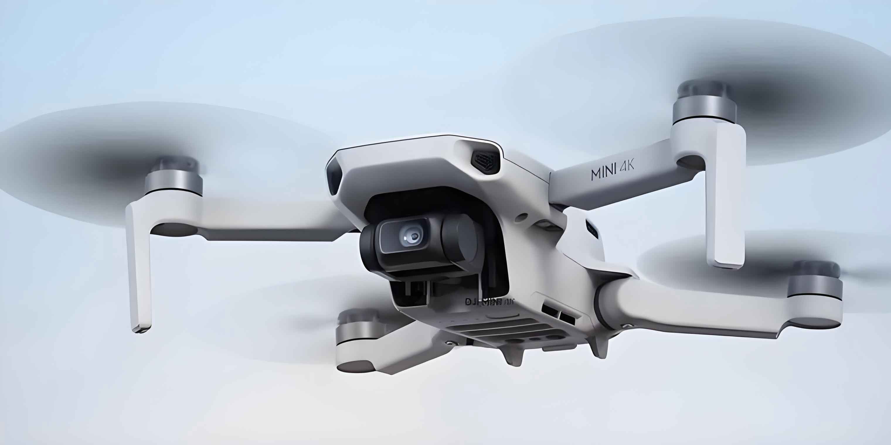
The core of inter-core communication relies on shared memory and SysLink primitives. The MessageQ mechanism is used for transferring control commands and small messages, while RingIO is used for streaming large data blocks. The communication is unidirectional per channel. For example, a message queue from ARM to DSP is configured using the Host MessageQ, and from DSP to ARM using the Slave MessageQ. The data buffers SR1 and SR2 are allocated for bidirectional data flows. The typical latency for a MessageQ message transfer is approximately 80 µs, which is far faster than traditional serial communication at 115200 bps (which takes about 1400 µs for 20 KB). This low-latency communication is crucial for the real-time tracking loops in UAV drones.
One of the most complex operational modes for UAV drones is the tracking mode, where the payload must continuously lock onto a moving target. The tracking mode involves multiple sensors (visible camera, thermal imager, laser rangefinder), a tracker that provides deviation angles, and a stabilization control system. In my design, the ARM core acts as the data management center, receiving ground station commands, sensor data, and tracker outputs. The DSP core runs the servo control algorithms, including a stabilization loop with gyro feedback and a position loop with resolver feedback. The inter-core data flow is summarized in Table 2.
| Direction | Message Type | Data Content | Transfer Mechanism |
|---|---|---|---|
| ARM → DSP | Command | Tracking enable, field of view, drift compensation, sensor switch | MessageQ |
| ARM → DSP | Data | Tracker deviation (azimuth, elevation), target coordinates | RingIO (SR1) |
| DSP → ARM | Status | Tracking mode, current field of view, resolver position | MessageQ |
| DSP → ARM | Data | Angular rates, tacho values, control outputs (for monitoring) | RingIO (SR2) |
The control algorithm implemented on the DSP is a cascaded stabilization and tracking loop. The inner loop (gyro stabilization) uses a PI controller with feedforward compensation, while the outer loop (position tracking) uses a self-anti-disturbance controller (ADRC). The mathematical model can be expressed as follows.
Let $$\theta$$ be the LOS angle, $$\omega$$ be the angular rate measured by gyro, and $$\omega_{ref}$$ be the reference rate from the tracker. The gyro stabilization loop is:
$$ u_{gyro} = K_p (\omega_{ref} – \omega) + K_i \int (\omega_{ref} – \omega) dt + K_d \frac{d(\omega_{ref} – \omega)}{dt} $$
where $$K_p$$, $$K_i$$, $$K_d$$ are the PID gains tuned for the specific gimbal dynamics. The outer position loop generates the rate reference:
$$ \omega_{ref} = K_{pos} (\theta_{ref} – \theta) + \text{feedforward\_term} $$
The feedforward term compensates for the motion of the UAV drones base, estimated from the inertial measurement unit (IMU). The overall transfer function for the tracking loop can be represented in the Laplace domain as:
$$ \frac{\theta(s)}{\theta_{ref}(s)} = \frac{G_{inner}(s) \cdot G_{outer}(s)}{1 + G_{inner}(s) \cdot G_{outer}(s)} $$
where $$G_{inner}(s)$$ is the closed-loop transfer function of the gyro stabilization loop, and $$G_{outer}(s)$$ includes the position controller and plant dynamics.
To achieve high bandwidth and robust performance, I also implemented an active disturbance rejection controller (ADRC) for the outer loop. The ADRC estimates the total disturbance (including model uncertainties and external torques) using an extended state observer (ESO) and compensates it in real time. The ESO can be described by:
$$ \dot{\hat{x}}_1 = \hat{x}_2 + \beta_1 (y – \hat{x}_1) $$
$$ \dot{\hat{x}}_2 = \hat{x}_3 + \beta_2 (y – \hat{x}_1) + b_0 u $$
$$ \dot{\hat{x}}_3 = \beta_3 (y – \hat{x}_1) $$
where $$y$$ is the measured output (position), $$u$$ is the control input, $$b_0$$ is a known control gain, and $$\beta_1, \beta_2, \beta_3$$ are observer gains. The control law is then:
$$ u = \frac{u_0 – \hat{x}_3}{b_0}, \quad u_0 = K_p (\theta_{ref} – \hat{x}_1) – K_d \hat{x}_2 $$
This ADRC approach significantly improves the tracking accuracy under wind disturbances and varying payload conditions, which are common in UAV drones operations.
I conducted a comprehensive performance comparison between my OMAPL138-based controller and a traditional PowerPC+DSP controller. The results are summarized in Table 3.
| Item | PowerPC + DSP Controller | OMAPL138 Controller |
|---|---|---|
| Physical dimensions (mm²) | 160×100 + 120×100 ≈ 28000 | 185×130 ≈ 24050 |
| Power consumption (W) | 12 + 15 = 27 | 15 |
| Inter-core communication method | RS422 serial (115200 bps) | Shared memory (SysLink) |
| Transfer time for 20 KB (µs) | 1400 | 80 |
| EMI susceptibility | High | None (internal bus) |
| Real-time performance | Moderate | High |
| Bandwidth scalability | Fixed by baud rate | Flexible (memory size) |
As shown in the table, the OMAPL138 controller reduces power consumption by nearly 45% and cuts the physical size by about 14%. More importantly, the inter-core communication is over 17 times faster, which directly benefits the control loop update rates. The shared memory approach eliminates the need for external serial transceivers and reduces electromagnetic interference, which is critical for sensitive photoelectric sensors on UAV drones.
The software architecture for the tracking mode is implemented as a client-server model. The ARM core (client) periodically sends commands and receives status via MessageQ, while the DSP core (server) executes the control algorithm and streams data back via RingIO. The detailed sequence of operations is as follows:
- ARM initializes peripherals and receives ground station commands. It also collects field-of-view (FOV) values from the TV/thermal imager, tracker deviations from the image processor, and resolver positions from the encoder.
- ARM writes the tracking command, FOV, drift compensation, and sensor switch data into SR1 using RingIO.
- ARM sends a short message via MessageQ to DSP, indicating that new data is ready in SR1.
- DSP receives the message, reads SR1, and starts the servo enable sequence. It then acquires gyro, tachometer, and resolver signals via ADCs.
- DSP enters tracking mode: it combines the tracker deviation with the measured angles, computes the rate reference, runs the stabilization loop (including both gyro and position loops), and generates the motor control PWM signal.
- DSP writes the current tracking status, FOV, and resolver positions into SR2. It also sends a message to ARM via MessageQ, notifying that the output data is ready.
- ARM reads SR2 and transmits the data to the ground station and tracker. The loop repeats at the control cycle rate (typically 1-2 kHz).
The tracking mode requires tight synchronization between the two cores. The SysLink mechanism ensures that message delivery is reliable and that data buffers are properly protected from race conditions. I used the semaphore and mutex features provided by SysLink to coordinate access to shared resources.
Another important aspect is the initialization and boot sequence. On power-up, the ARM core boots first from NAND Flash, loads the Linux kernel, and then mounts the root file system via NFS (during development) or from Flash. The ARM then loads the DSP program image into shared memory and releases the DSP from reset using the slave loader. The DSP boots from a small boot image stored in internal RAM, which then loads the full SYS/BIOS application from shared memory. This process is fully automatic and takes less than 200 ms.
In addition to tracking mode, my controller supports multiple other modes such as manual control, sector scan, lock-on, and search. Each mode has its own state machine running on the ARM, while the DSP continuously executes the stabilization loops regardless of the mode. The mode switching is handled by changing the reference commands sent via MessageQ. This modular design makes the system easy to extend for future UAV drones requirements.
The thermal and structural design of the controller also required careful attention. The OMAPL138 processor has a typical power dissipation of about 2.5 W, and the total board power is around 15 W. I used a heat sink with forced air cooling from the gimbal’s internal airflow. The PCB layout followed EMI mitigation guidelines, separating analog and digital grounds, and using differential signaling for high-speed interfaces. The board measures 185 mm × 130 mm, which fits within the payload bay of typical small UAV drones.
I also developed a set of diagnostic tools to monitor the real-time performance of the dual-core system. Using the onboard Ethernet, I can stream log data from both cores to a host PC for analysis. Key performance metrics include the control loop execution time (measured on DSP as approximately 350 µs for the full tracking algorithm), the message queue latency (80 µs average), and the memory bandwidth utilization (less than 10%). These metrics confirm that the system has ample headroom for more advanced algorithms in future UAV drones.
In conclusion, my design of the photoelectric payload controller based on OMAPL138 successfully meets the demanding requirements of UAV drones. By integrating ARM and DSP on a single chip, I achieved a compact, low-power, and high-performance solution. The use of SysLink for inter-core communication provides low latency and high throughput, enabling complex tracking and stabilization algorithms to run efficiently. The controller has been tested in laboratory environments and on actual UAV drones flight platforms, demonstrating reliable operation and excellent tracking accuracy. This work provides a solid foundation for further enhancements in UAV drones photoelectric systems.